- 您现在的位置:买卖IC网 > Sheet目录1214 > EVAL-ADE7878EBZ (Analog Devices Inc)BOARD EVAL FOR ADE7878
�� �
�
�ADE7854/ADE7858/ADE7868/ADE7878�
�MCU�
�INTERRUPT�
�Data� Sheet�
�t� 1�
�t� 2�
�t� 3�
�FLAG� SET�
�IRQx�
�PROGRAM�
�SEQUENCE�
�JUMP�
�TO� ISR�
�GLOBAL�
�INTERRUPT�
�MASK�
�CLEAR� MCU�
�INTERRUPT�
�FLAG�
�READ�
�STATUSx�
�WRITE�
�BACK�
�STATUSx�
�ISR� ACTION�
�(BASED� ON� STATUSx� CONTENTS)�
�ISR� RETURN�
�GLOBAL� INTERRUPT�
�MASK� RESET�
�JUMP�
�TO� ISR�
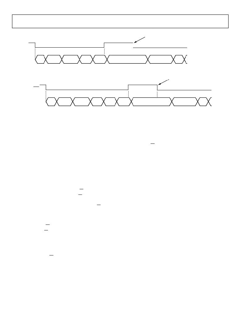
�Figure� 84.� Interrupt� Management�
�MCU�
�INTERRUPT�
�t� 1�
�t� 2�
�t� 3�
�FLAG� SET�
�IRQx�
�PROGRAM�
�SEQUENCE�
�JUMP�
�TO� ISR�
�GLOBAL�
�INTERRUPT�
�MASK�
�CLEAR� MCU�
�INTERRUPT�
�FLAG�
�READ�
�STATUSx�
�READ�
�PHx�
�WRITE�
�BACK�
�STATUSx�
�ISR� ACTION�
�(BASED� ON� STATUSx� CONTENTS)�
�ISR� RETURN�
�GLOBAL� INTERRUPT�
�MASK� RESET�
�JUMP�
�TO� ISR�
�Figure� 85.� Interrupt� Management� when� PHSTATUS,� IPEAK,� VPEAK,� or� PHSIGN� Registers� are� Involved�
�status� register� is� read� immediately� to� identify� the� phase� that�
�triggered� the� interrupt.� The� name,� PHx,� in� Figure� 85� denotes�
�one� of� the� PHSTATUS,� IPEAK,� VPEAK,� or� PHSIGN� registers.�
�Then,� STATUSx� is� written� back� to� clear� the� status� flag(s).�
�SERIAL� INTERFACES�
�The� ADE7854� /� ADE7858� /� ADE7868� /� ADE7878� have� three� serial�
�port� interfaces:� one� fully� licensed� I� 2� C� interface,� one� serial�
�peripheral� interface� (SPI),� and� one� high� speed� data� capture� port�
�(HSDC).� As� the� SPI� pins� are� multiplexed� with� some� of� the� pins�
�of� the� I� 2� C� and� HSDC� ports,� the� ADE78xx� accepts� two� confi-�
�gurations:� one� using� the� SPI� port� only� and� one� using� the� I� 2� C�
�port� in� conjunction� with� the� HSDC� port.�
�Serial� Interface� Choice�
�After� reset,� the� HSDC� port� is� always� disabled.� Choose� between�
�the� I� 2� C� and� SPI� ports� by� manipulating� the� SS/HSA� pin� after�
�power-up� or� after� a� hardware� reset.� If� the� SS/HSA� pin� is� kept�
�high,� then� the� ADE7854� /� ADE7858� /� ADE7868� /� ADE7878� use� the�
�I� 2� C� port� until� a� new� hardware� reset� is� executed.� If� the� SS/HSA�
�pin� is� toggled� high� to� low� three� times� after� power-up� or� after� a�
��use� the� SPI� port� until� a� new� hardware� reset� is� executed.� This�
�manipulation� of� the� SS/HSA� pin� can� be� accomplished� in� two�
�ways.� First,� use� the� SS/HSA� pin� of� the� master� device� (that� is,� the�
�microcontroller)� as� a� regular� I/O� pin� and� toggle� it� three� times.�
�Second,� execute� three� SPI� write� operations� to� a� location� in� the�
�address� space� that� is� not� allocated� to� a� specific� ADE78xx� register�
�(for� example� 0xEBFF,� where� eight� bit� writes� can� be� executed).�
�These� writes� allow� the� SS/HSA� pin� to� toggle� three� times.� See� the�
��involved.�
�After� the� serial� port� choice� is� completed,� it� needs� to� be� locked.�
�Consequently,� the� active� port� remains� in� use� until� a� hardware�
�reset� is� executed� in� PSM0� normal� mode� or� until� a� power-down.�
�If� I� 2� C� is� the� active� serial� port,� Bit� 1� (I2C_LOCK)� of� the� CONFIG2�
�register� must� be� set� to� 1� to� lock� it� in.� From� this� moment,� the�
��toggling� of� the� SS� pin� and� an� eventual� switch� into� using� the� SPI�
�port� is� no� longer� possible.� If� the� SPI� is� the� active� serial� port,� any�
�write� to� the� CONFIG2� register� locks� the� port.� From� this� moment,�
�a� switch� into� using� the� I� 2� C� port� is� no� longer� possible.� Once� locked,�
�the� serial� port� choice� is� maintained� when� the� ADE78xx� changes�
�PSMx� power� modes.�
�The� functionality� of� the� ADE78xx� is� accessible� via� several� on-�
�chip� registers.� The� contents� of� these� registers� can� be� updated� or�
�read� using� either� the� I� 2� C� or� SPI� interfaces.� The� HSDC� port� provides�
�the� state� of� up� to� 16� registers� representing� instantaneous� values� of�
�phase� voltages� and� neutral� currents,� and� active,� reactive,� and�
�apparent� powers.�
�I� 2� C-Compatible� Interface�
�The� ADE7854� /� ADE7858� /� ADE7868� /� ADE7878� supports� a� fully�
�licensed� I� 2� C� interface.� The� I� 2� C� interface� is� implemented� as� a� full�
�hardware� slave.� SDA� is� the� data� I/O� pin,� and� SCL� is� the� serial�
�clock.� These� two� pins� are� shared� with� the� MOSI� and� SCLK� pins�
�of� the� on-chip� SPI� interface.� The� maximum� serial� clock� frequency�
�supported� by� this� interface� is� 400� kHz.�
�The� two� pins� used� for� data� transfer,� SDA� and� SCL,� are� confi-�
�gured� in� a� wire-AND’ed� format� that� allows� arbitration� in� a�
�multimaster� system.�
�The� transfer� sequence� of� an� I� 2� C� system� consists� of� a� master� device�
�initiating� a� transfer� by� generating� a� start� condition� while� the� bus�
�is� idle.� The� master� transmits� the� address� of� the� slave� device� and�
�the� direction� of� the� data� transfer� in� the� initial� address� transfer.� If�
�the� slave� acknowledges,� the� data� transfer� is� initiated.� This� con-�
�tinues� until� the� master� issues� a� stop� condition,� and� the� bus�
�becomes� idle.�
�Rev.� H� |� Page� 68� of� 100�
�发布紧急采购,3分钟左右您将得到回复。
相关PDF资料
EVAL-ADE7880EBZ
BOARD EVAL FOR ADE7880
EVAL-ADE7953EBZ
BOARD EVAL FOR ADE7953
EVAL-ADF4002EBZ1
BOARD EVAL FOR ADF4002
EVAL-ADG788EBZ
BOARD EVALUATION FOR ADG788
EVAL-ADM1021AEB
BOARD EVAL FOR ADM1021
EVAL-ADM1023EB
BOARD EVAL FOR ADM1023
EVAL-ADM1031EB
BOARD EVAL FOR ADM1031
EVAL-ADM1062TQEBZ
BOARD EVALUATION FOR ADM1062TQ
相关代理商/技术参数
EVAL-ADE7880EBZ
功能描述:BOARD EVAL FOR ADE7880 RoHS:是 类别:编程器,开发系统 >> 评估演示板和套件 系列:* 产品培训模块:Obsolescence Mitigation Program 标准包装:1 系列:- 主要目的:电源管理,电池充电器 嵌入式:否 已用 IC / 零件:MAX8903A 主要属性:1 芯锂离子电池 次要属性:状态 LED 已供物品:板
EVAL-ADE7880EBZ
制造商:Analog Devices 功能描述:ADE7880, ENERGY METER, 3 PH, SPI, I2C, E
EVAL-ADE7913EBZ
制造商:AD 制造商全称:Analog Devices 功能描述:3-Channel, Isolated, Sigma-Delta ADC with SPI
EVAL-ADE7953EBZ
功能描述:BOARD EVAL FOR ADE7953 RoHS:是 类别:编程器,开发系统 >> 评估演示板和套件 系列:- 标准包装:1 系列:PSoC® 主要目的:电源管理,热管理 嵌入式:- 已用 IC / 零件:- 主要属性:- 次要属性:- 已供物品:板,CD,电源
EVAL-ADF4001EBZ2
制造商:Analog Devices 功能描述:Evaluation Board For Pll Frequency Synthesizer 制造商:Analog Devices 功能描述:ADF4001 PLL SYNTHESIZER EVAL BOARD
EVAL-ADF4002EB1
制造商:Analog Devices 功能描述:EVAL BOARD - Bulk
EVAL-ADF4002EBZ1
功能描述:BOARD EVAL FOR ADF4002 RoHS:是 类别:编程器,开发系统 >> 评估演示板和套件 系列:- 产品培训模块:Obsolescence Mitigation Program 标准包装:1 系列:- 主要目的:电源管理,电池充电器 嵌入式:否 已用 IC / 零件:MAX8903A 主要属性:1 芯锂离子电池 次要属性:状态 LED 已供物品:板
EVAL-ADF4007EBZ1
功能描述:BOARD EVALUATION FOR ADF4007EB1 RoHS:是 类别:编程器,开发系统 >> 评估演示板和套件 系列:- 标准包装:1 系列:PSoC® 主要目的:电源管理,热管理 嵌入式:- 已用 IC / 零件:- 主要属性:- 次要属性:- 已供物品:板,CD,电源